Difference between revisions of "User:DustyFB/Sandbox/Device:Memory Relay"
| (One intermediate revision by the same user not shown) | |||
| Line 2: | Line 2: | ||
|ru=Реле памяти | |ru=Реле памяти | ||
|ua=Реле пам'яті | |ua=Реле пам'яті | ||
}}{{ | }}{{SB Infobox Begin | ||
|{{ | |{{SB Infobox Header | ||
|image=[[Image:Memory_relay.png]] | |image=[[Image:Memory_relay.png]] | ||
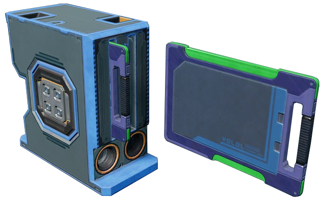
|caption=A memory relay, and associated memory chip | |caption=A memory relay, and associated memory chip | ||
| Line 9: | Line 9: | ||
|border=none | |border=none | ||
}} | }} | ||
|{{ | |{{SB Infobox Device General Information | ||
|type=YOLOL device | |type=YOLOL device | ||
|function=Storing YOLOL data | |function=Storing YOLOL data | ||
| Line 19: | Line 19: | ||
}} | }} | ||
|{{ | |{{SB Infobox Device IO | ||
|electricIn=Passive | |electricIn=Passive | ||
|sockets=4 | |sockets=4 | ||
| Line 25: | Line 25: | ||
|modInterfaces=2 | |modInterfaces=2 | ||
}} | }} | ||
|{{ | |{{SB Infobox Section Header|Extra Characteristics}} | ||
|{{ | |{{SB Infobox Section | ||
|Test1=yup | |Test1=yup | ||
|Test2=nup | |Test2=nup | ||
|Test3=kyllä | |Test3=kyllä | ||
}} | }} | ||
|{{ | |{{SB Infobox Device Construction | ||
|bastium=45% | |bastium=45% | ||
|corazium=10% | |corazium=10% | ||
|vokarium=25% | |vokarium=25% | ||
|ilmatrium=20% | |ilmatrium=20% | ||
}} | }} | ||
| Line 72: | Line 72: | ||
* [[Data networks|Data networks]] | * [[Data networks|Data networks]] | ||
* [[YOLOL|YOLOL]] | * [[YOLOL|YOLOL]] | ||
Latest revision as of 11:05, 21 May 2021
The memory relay is a device used to transfer data fields from one memory chip to another, allowing for device fields to be linked with different field names. Memory relays separate sub-networks allowing for one-way broadcasting of variable changes, enabling the creation of modular YOLOL systems.
Basic information
Memory Relays are connected to two separate data networks via cable sockets at both ends of the device, or via a connection to modular device racks. Facing the device's 'front' (where the memory chips are inserted):
- The left side of the relay acts as the "input" connection.
- The right side of the relay acts as the "output" connection.
When the relay is powered, changes made to device fields on the input chip will propagate to the corresponding device field on the output chip. Data which occupies a device field on the left side of the relay will be propagated to the device field with a matching index on the right side of the relay. For example: The data in device field #3 on the input (left) chip will be automatically propagated to device field #3 on the output (right) chip. However, both sides of the relay must be enabled for the data to propagate: Disabling either side will prevent this transfer.
- Values between networks are not automatically synchronized.
- This means that connected networks may contain different values for similarly named device fields.
Device fields
The memory relay has two distinct sub-components which have unique device fields, as the left and right side of the device. These device fields can only be accessed by interacting with the appropriate sub-component.
| YOLOL field | Description | Range |
|---|---|---|
| IsMasterEnabled | On / Off, left side | 0 / 1 |
| IsEnabled | On / Off, right side | 0 / 1 |
To learn more about how to use fields, consult these wiki pages:
